| icon |
|---|
material/cog |
The circuit board dimensions are illustrated in the drawing below; the measurements are in inches.
[{ width=750 }](./assets/board_files/dimensions.png "Click to enlarge") [Dimensions (PDF)](./assets/board_files/dimensions.pdf) of the RA6M5 Thing Plus, in inches.??? tip "Need more measurements?" For more information about the board's dimensions, users can download the Eagle files for the board. These files can be opened in Eagle and additional measurements can be made with the dimensions tool.
??? info ":octicons-download-16:{ .heart } Eagle - Free Download!"
Eagle is a [CAD]("computer-aided design") program for electronics that is free to use for hobbyists and students. However, it does require an account registration to utilize the software.
<center>
[Download from<br>:autodesk-primary:{ .autodesk }](https://www.autodesk.com/products/eagle/free-download "Go to downloads page"){ .md-button .md-button--primary width="200px" }
</center>
??? info ":straight_ruler: Dimensions Tool"
This video from Autodesk demonstrates how to utilize the dimensions tool in Eagle, to include additional measurements:
<center>
<div class="video">
<iframe src="https://www.youtube.com/embed/dZLNd1FtNB8" title="EAGLE Dimension Tool" frameborder="0" allow="accelerometer; autoplay; clipboard-write; encrypted-media; gyroscope; picture-in-picture" allowfullscreen></iframe>
{ .qr width=100 }
</div>
</center>
The USB-C connector is used to provide power and program the board. For most users, it will also be the primary programming interface for the RA6M5 Thing Plus.
[{ width=750 }](./assets/img/hookup_guide/USB.png "Click to enlarge") USB-C connector on the RA6M5 Thing Plus.The RA6M5 Thing Plus only requires 3.3V to power the board. However, the simplest method to power the board is through the USB-C connector. Alternatively, the 3V3, VBAT, and VUSB pins can also be used to supply power to the board.
flowchart LR
	A[USB-C] === B(("`**VUSB**`")) ===> |VUSB > VBAT| Switch;

	subgraph Battery Charger
		direction LR
		C[MCP73831] -.-> D[LiPo Battery];
	end

	subgraph Switch
		F[LM66200];
	end

	B ==> C;
	D === E(("`**VBAT**`")) == VBAT > VUSB ==> Switch;

	F ===	H[RT9080] ==> I(("`**3V3**`"));
	F === G[RT9080] ==> J(("`**VREF**`"));

	click B "#vusb"
	click C "#charging-circuit"
	click E "#vbat"
	click F "#power-control"
	click J "#vref"
	click I "#3v3"
Below, is a summary of the power circuitry for this board:
=== ":material-power: 3V3"
* Primary power for the RA6M5 Thing Plus
* Powers the RA6M5 module, DA14531MOD, QSPI flash, µSD card slot, Qwiic connector, WS2812 RGB LED, and power LED
* A regulated 3.3V is provided by an RT9080 LDO from VUSB or VBAT
* The output voltage from the RT9080 is controlled by the EN pin on the board
* The RT9080 can source up to 600mA of current, which is only limited by the power source from the LM66200 switch
* The power source from the LM66200 is automatically switched between VUSB or VBAT, based on which has the greater voltage
* As an input, it requires a regulated 3.3V to avoid contention with the LDO regulator
!!! info "<span style="font-weight: 400;">The input voltage range for the RT9080 is 1.2-5.5V</span>"
=== ":material-usb-port: VUSB"
* Usually powered through the USB-C connector (5V)
* Input voltage range: 3.75 - 5V
* The maximum voltage is limited by the ideal diode switch at 5.5V (1.6-5.5V)
* The minimum voltage is limited by the charge controller at 3.75V (3.75-6V)
* Primary power source for the RT9080 LDOs when VUSB > VBAT; via the LM66200 ideal diode switch
* Powers the MCP73831 linear charge management controller
* Provides a 213mA (max) rate of charge to a connected battery
=== ":material-battery-charging: VBAT"
* The voltage from the JST battery connector; is meant for single-cell LiPo batteries
* A connected battery will be charged by the MCP73831 charge controller, when sufficient power is provided from VUSB
* Primary power source for the RT9080 LDOs when VBAT > VUSB; via the LM66200 ideal diode switch
* A battery's charge can be monitored through the MAX17048 fuel gauge
=== ":material-sine-wave: :material-gauge: VREF"
* The analog reference voltage for the RA6M5 module's ADC and DAC channels
* Provided by a RT9080 LDO regulator, separate from one providing the 3V3 power supply
!!! info "<span style="font-weight: 400;">The input voltage range for the RT9080 is 1.2-5.5V</span>"
=== ":material-format-line-style: GND"
* The common ground or the 0V reference for the voltage supplies
=== ":material-connection: Qwiic Connector"
* The 4-pin JST connector provides a regulated 3.3V voltage to peripheral Qwiic devices from 3V3
??? info "Detailed Diagram"
<center>

```mermaid

flowchart LR
	D === E(("`**VBAT**`")) == VBAT > VUSB ==> Switch;
	A[USB-C] === B(("`**VUSB**`")) == VUSB > VBAT ==> Switch;
	C --- T[CHG LED];

subgraph Battery Charger
		C[MCP73831] -.-> D[LiPo<br>3.5-4.2V]
	end

	subgraph Switch
		S[LM66200];
		S === I[RT9080] & H[RT9080];
	end

	subgraph Powered_Components
		L[PWR LED];
		M[RA6M5] --- N[DA14531MOD];
		M --- O[QSPI Flash];
		M --- P[SD Card];
		M --- Q[WS2812 LED];
		M --- I2C;
		subgraph I2C
			R[Qwiic Connector];
			F[MAX17048];
		end
	end

	B ==> C;
	B ====> T;
	I --- U(("`**EN**`"));
	I ==> K(("`**3V3**`")) === Powered_Components;
	H ==> J(("`**VREF**`")) --> M;
	H --- W(("`**D37**`")) --- M;
	D ------ F;
	Switch --- V(("`**D38**`")) --- M;
```

</center>
For more details, users can reference the schematic and the datasheets of the individual components in the power circuitry.
The red, PWR LED will light up once 3.3V is supplied to the board; however, for most users, it will light up when 5V is supplied through the USB connection or when a LiPo battery is connected to the JST connector.
The charging circuit utilizes the MCP73831 linear charge management controller from Microchip Technologies, which is powered by the USB-C connector or VUSB. The controller provides a 213mA charge rate for a LiPo battery connected to the JST connector. Active charging is indicated by the yellow, CHG LED. If the charge controller is shut down or charging is complete, the CHG LED will turn off. The board also includes a MAX17048 fuel gauge from Analog Devices to monitor the charge left on the battery.
flowchart LR
	A[USB-C] === B(("`**VUSB**`")) ==> C & G;
	D ===> E(("`**VBAT**`"));
	D --- F[MAX17048] === H(("`**3V3**`"));
	G[CHG LED] --- C[MCP73831];

	subgraph Battery Charger
		C -.-> |213mA| D[LiPo<br>3.5-4.2V];
	end
For more details, please refer to the MCP73831 and MAX17048 datasheets, schematic, and the Status LEDs and Battery Fuel Gauge sections below.
The primary power source for the RT9080 LDO regulators is automatically switched between VUSB and VBAT by the LM66200 ideal diode switch; based on their voltage levels. This will be indicated by the ST pin of the LM66200, which is connected to the P001 GPIO (D38) of the RA6M5. A LOW state will indicate that power is being supplied from VUSB (or the USB-C connector); while a HIGH state will indicate power is being drawn from VBAT (or the battery JST connector).
flowchart LR
	A[USB-C] === B(("`**VUSB**`")) == VUSB > VBAT ==> Switch;
	U(("`**D38**`")) --- Switch;
	D[LiPo] === E(("`**VBAT**`")) == VBAT > VUSB ==> Switch;

	subgraph Switch
		S[LM66200];
	end

	S === H[RT9080] ===> J(("`**3V3**`"));
	H --- T(("`**EN**`"));
	I --- V(("`**D37**`"));
	S === I[RT9080] ===> K(("`**VREF**`"));
The 3.3V regulated output from the primary RT9080 is enabled by default and controlled by the EN pin on the board. Meanwhile, the voltage output from the RT9080 for the analog reference voltage (VREF) of the RA6M5 is controlled by its P500 GPIO (D37). Users can disable the 3.3V power output of either of the RT9080 LDO regulators, by setting the associated control pin LOW.
For more details, please refer to the LM66200 datasheet, RT9080 datasheet, and schematic.
The brains of the board is the RA6M5 microcontroller from Renesas, a low-power Arm^®^ Cortex^®^-M33 processor with a clock speed up to 200Mhz, 512kB of SRAM, and 2MB of flash memory. This high-performance microcontroller features an extensive list of peripheral capabilities and is perfect for real-time applications.
- Arm^®^ Cortex^®^-M33 Core
- Clock Frequency: 200MHz
- Flash Memory: 2MB (code); 8kB (data)
- SRAM: 512kB w/ ECC Support
- Arm Memory Protection Unit (Arm MPU)
- Secure Crypto Engine
- Two Watchdog Timers (WDT)
- Operating Voltage: 3.0V to 3.6V
- Current Consumption:
- Maximum: 143mA
- Normal: 32mA
- Sleep: 11mA
- Deep Sleep: 0.9-131µA
- Current Consumption:
- Operating modes:
- Single-chip or SCI/USB boot
- Operating Temperature: -40 to 85 °C
- 75 GPIO Pins
- RTC with Calendar
- CRC Calculator
- Internal Temperature Sensor
Peripherals
- 12-bit ADC (x6)
- 12-bit DAC (x2)
- 32-bit PWM Channels (x4)
- 16-bit PWM Channels (x6)
- UART (x10)
- I^2^C Bus (x3)
- SPI Bus (x2)
- QSPI (x1)
- SD/MMC Host Interface
{--
- OSPI (x1)
- CAN Interface
- USB 2.0 (Full/High Speed)
- Ethernet MAC/DMA Controller
- Serial Sound Interface Enhanced
- Consumer Electronics Control
- Capacitive Touch Sensing
--}
!!! warning "Note" Users should be aware that not all of the features, listed above, will be available in the Arduino IDE.
??? success "DFU Mode" If users are having issues uploading code to the board, the RA6M5 can be manually forced into DFU mode. This issue, often occurs when the USB connection is busy and a reset can't be triggered on the RA6M5, to initialize the upload process. To force the RA6M5 Thing Plus into DFU mode:
1. Double-tap the ++"RST"++ button
	- The `STAT` LED should be fading in/out very slowly
1. Users should now, be able to upload a new program
	- It shouldn't be necessary to select a COM port in the Arduino IDE; only the board needs to be selected
1. Once programming is complete, the MCU should reboot on its own. Otherwise:
	- Press the ++"RST"++ button
	- Power cycle the board
For more technical specifications for the RA6M5 microcontroller, please refer to the RA6M5 datasheet and RA6M5 user manual.
Debug pins are available for the RA6M5, as 0.1" test points on the board. However, the debugging feature is only available through the Renesas FSP (not covered in this tutorial).
=== "SWD"
<center>
	<table border="1" markdown>
		<tr markdown>
			<td style="text-align:center" markdown>**GND**</td>
			<td style="text-align:center" markdown>**SWCLK**</td>
			<td style="text-align:center" markdown>**3.3V**</td>
			<td style="text-align:center" markdown>**|**</td>
		</tr>
		<tr markdown>
			<td style="text-align:center" markdown>**RST**</td>
			<td style="text-align:center" markdown>**SWO**</td>
			<td style="text-align:center" markdown>**SWDIO**</td>
		</tr>
	</table>
</center>
=== "JTAG"
<center>
	<table border="1" markdown>
		<tr markdown>
			<td style="text-align:center" markdown>**GND**</td>
			<td style="text-align:center" markdown>**TCK**</td>
			<td style="text-align:center" markdown>**3.3V**</td>
			<td style="text-align:center" markdown>**|**</td>
		</tr>
		<tr markdown>
			<td style="text-align:center" markdown>**RST**</td>
			<td style="text-align:center" markdown>**TDO**</td>
			<td style="text-align:center" markdown>**TMS**</td>
		</tr>
	</table>
</center>
!!! info "Pin Connections" In case users are interested, these are the pin connections of the debugging test points for the RA6M5. For more details, please reference the schematic and Eagle files.
- `TMS`/`SWDIO`: `P108`
- `TCK`/`SWCLK`: `P300`
- `TDO`/`SWO`: `P109`
- {--`TDI`: `P110` (POCI/`D17`)--} ***(Not a JTAG test point)***
!!! note In order to debug the RA6M5, users will need a debug probe. We recommend the J-Link debug probes from Segger. However, users should verify the supported devices before purchasing these products; for example, we had a few issues with the J-Link EDU Mini.
For more details, please refer to the schematic and RA6M5 datasheet.
While there are 75 GPIO pins that are available on the RA6M5, only 44 GPIO pins are utilized with the RA6M5 Thing Plus. Additionally, of those 44 GPIO, only 21 GPIO pins are broken out into the PTH breakout pins. The breakout pins are in a Feather form-factor layout with a 0.1" pitch spacing to make them compatible with standard headers and Feather shields/wings.
Some of the RA6M5's peripheral capabilities may be inaccessible to users with the available 44 GPIO. However, any of the available GPIO pins can operate as digital I/O; with several of these pins featuring additional peripheral support. The pins utilized by the RA6M5 Thing Plus, along with their capabilities, are summarized in our graphical datasheet and detailed in the sections below.
[:material-download:{ .heart } Download the Graphical Datasheet{ .tinyqr }](./assets/board_files/graphical_datasheet.pdf "Click to download the graphical datasheet"){ .md-button .md-button--primary }
!!! arduino "Board Limitations" Users should be aware that some of the features of the RA6M5 may not be available in the Arduino IDE. This is due to either the lack of support in the Renesas-Arduino core and/or pins that are unavailable on the RA6M5 Thing Plus. For the full capabilities of the RA6M5, the Renesas FSP should be utilized.
<div class="grid" markdown>

<div markdown>

- Only one I<sup>2</sup>C bus is defined.
- Only three UART interfaces are defined.
	- `Serial` - UART (USB)
	- `Serial1` - `RX`/`TX` GPIO Pins
	- `Serial2` - DA14531MOD UART
- Only one SPI bus is defined.

</div>


<div markdown>

!!! warning "Note"
	- All the GPIO on the RA6M5 Thing Plus are :high_voltage: **3.3V** pins
	- While the datasheet specifies there are fourteen 5V-tolerant I/O pins; most of the exposed pins are **not 5V-tolerant**! To interface with higher voltage components, a [**logic-level adapter**](https://learn.sparkfun.com/tutorials/147) should be utilized.

</div>

</div>
=== ":material-square-wave: Digital I/O"
Any GPIO pin on the RA6M5 Thing Plus can operate as a digital I/O (input or output). To access this functionality in the Arduino IDE, users must first declare the pin operation in their #!cpp setup() loop, using the #!cpp pinMode(pin, mode) function.
**Input**

:	If a pin is configured as an `INPUT`, the microcontroller can monitor if the pin's state is **HIGH** or **LOW**. As **Input** pins are **High Impedance**, it takes very little current to move the input pin from one state to another.

	!!! arduino
		In the Arduino IDE, this is accessed through the [`#!cpp digitalRead(pin)` function](https://www.arduino.cc/reference/en/language/functions/digital-io/digitalread/), which returns a `HIGH` or `LOW` value.

**Output**

:	If a pin is configured as an `OUTPUT`, the microcontroller can provide a **HIGH** or **LOW** voltage output from the pin. As **Output** pins are **Low Impedance**, they can provide a certain amount of current for other circuits.

	!!! arduino
		In the Arduino IDE, this is accessed through the [`#!cpp digitalWrite(pin, value)` function](https://www.arduino.cc/reference/en/language/functions/digital-io/digitalwrite/) and providing a `HIGH` or `LOW` value.

	!!! warning
		There are electrical limitations to the amount of current that I/O pins can sink or source. For more details, check out the [RA6M5 datasheet](https://www.renesas.com/us/en/document/dst/ra6m5-group-datasheet?r=1493931).

!!! tip "Tip - Creating a PWM Output"
	A digital output pin can only either be fully on **HIGH** or fully off **LOW**. By turning a digital pin's output, on and off very quickly with precise timings, the average voltage can be controlled and emulate an analog output. This method is called [PWM](https://docs.arduino.cc/learn/microcontrollers/analog-output/).

	*Please refer to the [PWM Outputs](#pwm-outputs) tab for more instructions or check out this great [tutorial](https://learn.sparkfun.com/tutorials/pulse-width-modulation) to learn more about pulse width modulation.*
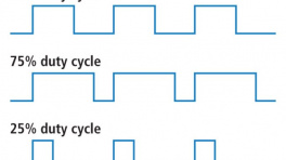
=== ":material-square-wave: PWM Outputs"
The RA6M5 supports up to four 32-bit and six 16-bit PWM (Pulse Width Modulation) channels on most of its GPIO pins. A PWM output will produce a square waveform with a variable duty cycle, a ratio of time a signal is HIGH for a given wave period. In the Arduino IDE, this feature is accessed using the #!cpp analogWrite(pin, value) function, where the desired duty cycle is specified as an 8-bit value.
$$
\operatorname{Duty-Cycle}=\frac{value_{\operatorname{(8-bit)}}}{255_{(\operatorname{8-bit})}} = \frac{time_{HIGH}}{time_{Total}}=\frac{t_{HIGH}}{t_{LOW} + t_{HIGH}}
$$
<div class="grid" markdown>
<div markdown>
<figure markdown>
[{ width=200 }](./assets/img/hookup_guide/pins-pwm.png "Click to enlarge")
<figcaption markdown>The GPIO pins that support PWM outputs on the RA6M5 Thing Plus.</figcaption>
</figure>
</div>
<div markdown>
??? warning "Mean Value ≠ Analog"
PWM signals are often mistaken for analog signals; however, a PWM output is not a **true** analog signal. These signals can *emulate an analog output*, based on the average voltage output of their square waveform for a specific duration of time.
!!! arduino
By default, in the Arduino IDE, `analogWrite()` accepts an 8-bit value. To change the resolution of the PWM signal for the `#!cpp analogWrite()` function, use the [`#!cpp analogWriteResolution(bits)` function](https://www.arduino.cc/reference/en/language/functions/zero-due-mkr-family/analogwriteresolution/).
*A PWM output is not a true analog signal. For a true analog output, please refer to the [**Analog Outputs** tab](#analog-outputs).*
!!! tip
To learn more about pulse width modulation (PWM), check out this great [tutorial](https://learn.sparkfun.com/tutorials/51).
<div class="grid cards" markdown align="center">
- <a href="https://learn.sparkfun.com/tutorials/51">
<figure markdown>
</figure>
---
**Pulse Width Modulation**</a>
</div>
</div>
</div>
=== ":material-sine-wave: Analog Inputs"
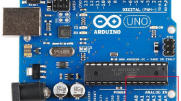
The RA6M5 has six 12-bit ADC channels on its GPIO pins to read analog signals. This functionality is accessed in the Arduino IDE using the #!cpp analogRead(pin) function. The available ADC pins are highlighted in the image below.
<div class="grid" markdown>
<div markdown>
<figure markdown>
[{ width=200 }](./assets/img/hookup_guide/pins-adc.png "Click to enlarge")
<figcaption markdown>Analog input pins on the RA6M5 Thing Plus.</figcaption>
</figure>
</div>
<div markdown>
!!! arduino
In the Arduino IDE, `#!cpp analogRead()` returns a 10-bit value by default. To change the resolution of the value returned by the `#!cpp analogRead()` function, use the [`#!cpp analogReadResolution(bits)` function](https://www.arduino.cc/reference/en/language/functions/zero-due-mkr-family/analogreadresolution/).
!!! tip
To learn more about analog vs. digital signals, check out this great [tutorial](https://learn.sparkfun.com/tutorials/35).
<div class="grid cards" markdown align="center">
- <a href="https://learn.sparkfun.com/tutorials/35">
<figure markdown>
</figure>
---
**Analog to Digital Conversion**</a>
</div>
</div>
</div>
=== ":material-sine-wave: Analog Outputs"
The RA6M5 has two 12-bit DAC channels on its GPIO pins to output analog signals. This feature is accessed in the Arduino IDE using the #!cpp AnalogWave library from the Renesas Arduino core. The available DAC pins are highlighted in the image below.
<div class="grid" markdown>
<div markdown>
<center>
| GPIO Pin | DAC Channel |
| :------: | :---------- |
| `A0` | `DAC` |
| `A1` | `DAC1` |
</center>
<figure markdown>
[{ width=200 }](./assets/img/hookup_guide/pins-dac.png "Click to enlarge")
<figcaption markdown>Analog (DAC) output pins on the RA6M5 Thing Plus.</figcaption>
</figure>
</div>
<div markdown>
!!! arduino
When implementing the `AnalogWave` library, users will need to link the library and create an instance of the `analogWave` class with a DAC `pin` declared for the output.
```c++
#include "analogWave.h" // Include the library for analog waveform generation
analogWave wave(pin); // Create an instance of the analogWave class, using a DAC pin
```
*For more information, please refer to the [Analog I/O example](../example-analog/#analogwave-library) in this guide.*
!!! tip
To learn more about analog vs. digital signals, check out this great [tutorial](https://learn.sparkfun.com/tutorials/89).
<div class="grid cards" markdown align="center">
- <a href="https://learn.sparkfun.com/tutorials/89">
<figure markdown>
</figure>
---
**Analog vs. Digital**</a>
</div>
</div>
</div>
=== "Serial Pins"
The RA6M5 supports up to ten UART ports. However, only the three UART ports are predefined in the Renesas Arduino core. In the Arduino IDE, the serial communication class is used for the USB connection (#!cpp Serial), the labeled UART I/O pins on the board (#!cpp Serial1), and UART connection to the DA14531MOD (#!cpp Serial2).
<div class="grid" markdown>
<div markdown>
<figure markdown>
[{ width=200 }](./assets/img/hookup_guide/pins-serial.png "Click to enlarge")
<figcaption markdown>UART connections on the RA6M5 Thing Plus.</figcaption>
</figure>
</div>
<div markdown>
!!! arduino
By default, in the Arduino IDE, the RA6M5 Thing Plus board definition supports:
<center>
| Arduino Object | GPIO Pins | Connection |
| :------------- | :---------- | :--------: |
| `Serial` | | **USB** |
| `Serial1` | **RX** - `P408` *(`D21`)*<br>**TX** - `P409` *(`D20`)* | PTH Pins |
| `Serial2` | **RX** - `P601` *(`D32`)*<br>**TX** - `P602` *(`D31`)*<br>**RTS** - `P301` *(`D33`)*<br>**CTS** - `P303` *(`D34`)* | **DA14531MOD**<br>*Bluetooth Module* |
</center>
To utilize serial communication on other pins, users will need to create a custom serial port object and declare which pins to access.
??? warning "Shared UART Port"
Users should be aware that the UART port for pins `D17`/`D18`, **UART9**, is also utilized for communication with the DA14531MOD Bluetooth module. Therefore, if **UART9** is already being utilized for the DA14531MOD; the UART port will be unavailable on pins `D17`/`D18`.
<center>
| UART Port | Arduino Object | GPIO Pins | Connection |
| :-------: | :------------- | :---------- | :--------: |
| **USB** | `Serial` | | **USB** |
| **UART3** | `Serial1` | **RX** - `P408` *(`D21`)*<br>**TX** - `P409` *(`D20`)* | PTH Pins |
| **UART9** | `Serial2` | **RX** - `P601` *(`D32`)*<br>**TX** - `P602` *(`D31`)*<br>**RTS** - `P301` *(`D33`)*<br>**CTS** - `P303` *(`D34`)* | **DA14531MOD**<br>*Bluetooth Module* |
| **UART9** | | **RX** - `P110` *(`D17`)*<br>**TX** - `P109` *(`D18`)* | PTH Pins |
| **UART7** | | **RX** - `P402` *(`D05`)*<br>**TX** - `P401` *(`D15`)*<br>**RTS** - `P403` *(`D04`)*<br>**CTS** - `P404` *(`D03`)* | PTH Pins |
</center>
!!! tip
To learn more about serial communication, check out this great [tutorial](https://learn.sparkfun.com/tutorials/8).
<div class="grid cards" markdown align="center">
- <a href="https://learn.sparkfun.com/tutorials/8">
<figure markdown>
</figure>
---
**Serial Communication**</a>
</div>
</div>
</div>
=== "SPI Pins"
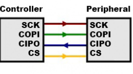
The RA6M5 supports up to two SPI buses. However, only a single SPI port is defined in the Renesas Arduino core. In the Arduino IDE, the SPI communication class is configured to utilize pins SCK - P111/D19, POCI - P110/D17, PICO - P109/D18, and P112/D0 for its chip select.
??? note "New Nomenclature"
To comply with the latest [OSHW](https://www.oshwa.org/) design practices, we have [adopted the new SPI signal nomenclature](https://www.sparkfun.com/spi_signal_names) (`SDO`/`SDI` and `PICO`/`POCI`). The terms **Master** and **Slave** are now referred to as **Controller** and **Peripheral**. The `MOSI` signal on a controller has been replaced with `SDO` or `PICO`. Please refer to this [announcement on the decision to deprecate the `MOSI`/`MISO` terminology and transition to the `SDO`/`SDI` naming convention](https://www.oshwa.org/a-resolution-to-redefine-spi-signal-names).
<div class="grid" markdown>
<div markdown>
<figure markdown>
[{ width=200 }](./assets/img/hookup_guide/pins-spi.png "Click to enlarge")
<figcaption markdown>SPI pins on the RA6M5 Thing Plus.</figcaption>
</figure>
</div>
<div markdown>
!!! arduino
By default, in the Arduino IDE, the RA6M5 Thing Plus board definition supports:
<center>
| SPI Pin | GPIO |
| :-----: | :--------------- |
| POCI | `P110` *(`D17`)* |
| PICO | `P109` *(`D18`)* |
| SCK | `P111` *(`D19`)* |
| CS | `P112` *(`D0`)* |
</center>
To utilize SPI communication on other pins, users will need to create a custom SPI object and declare which pins to access.
!!! tip
To learn more about the serial peripheral interface (SPI) protocol, check out this great [tutorial](https://learn.sparkfun.com/tutorials/16).
<div class="grid cards" markdown align="center">
- <a href="https://learn.sparkfun.com/tutorials/16">
<figure markdown>
</figure>
---
**Serial Peripheral Interface (SPI)**</a>
</div>
</div>
</div>
=== "I^2^C Pins"
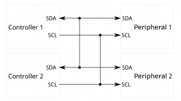
The RA6M5 supports up to three I^2^C buses. However, only a single I^2^C bus is defined in the Renesas Arduino core. In the Arduino IDE, the Wire class is configured to utilize the SDA - P401/D15 and SCL -P400/D16 pins. These pins also share the same I^2^C bus as the Qwiic connector and MAX17048 fuel gauge.
<div class="grid" markdown>
<div markdown>
<figure markdown>
[{ width=200 }](./assets/img/hookup_guide/pins-i2c.png "Click to enlarge")
<figcaption markdown>I^2^C connections on the RA6M5 Thing Plus.</figcaption>
</figure>
</div>
<div markdown>
!!! arduino
By default, in the Arduino IDE, the RA6M5 Thing Plus board definition supports:
<center>
| I^2^C Pin | GPIO |
| :-------: | :--------------- |
| SCL | `P400` *(`D16`)* |
| SDA | `P401` *(`D15`)* |
</center>
To utilize the I^2^C ports on other pins, users will need to create a custom Wire object and declare which pins to access.
!!! tip
To learn more about the inter-integrated circuit (I^2^C) protocol, check out this great [tutorial](https://learn.sparkfun.com/tutorials/82).
<div class="grid cards" markdown align="center">
- <a href="https://learn.sparkfun.com/tutorials/82">
<figure markdown>
</figure>
---
**I2C**</a>
</div>
</div>
</div>
??? tip "What is Qwiic?"
<div class="grid" markdown>
<div markdown>
<!-- Qwiic Banner -->
<center>
[{ width=400 }](https://www.sparkfun.com/qwiic)
[{ width=400 }](https://www.sparkfun.com/qwiic)
</center>
---
The [Qwiic connect system](https://www.sparkfun.com/qwiic) is a solderless, polarized connection system that allows users to seamlessly daisy chain I^2^C boards together. Play the video, to learn more about the Qwiic connect system or click on the banner above to learn more about [Qwiic products](https://www.sparkfun.com/qwiic).
</div>
<div style="max-height=400px;" markdown>
<center>
<div class="video-container">
<iframe src="https://www.youtube.com/embed/x0RDEHqFIF8" title="SparkFun's Qwiic Connect System" frameborder="0" allow="accelerometer; encrypted-media; gyroscope; picture-in-picture" allowfullscreen></iframe>
{ .qr width=100 }
</div>
</center>
</div>
</div>
!!! info "Features of the Qwiic System"
=== "No Soldering"
{ align="left" width="90" }
{ align="left" width="90" }
Qwiic cables (4-pin JST) plug easily from development boards to sensors, shields, accessory boards and more, making easy work of setting up a new prototype.
=== "Polarized Connector"
{ align="left" width="90" }
{ align="left" width="90" }
There's no need to worry about accidentally swapping the `SDA` and `SCL` wires on your breadboard. The Qwiic connector is polarized so you know you’ll have it wired correctly every time.
The part numbers for the PCB connector is `SM04B-SRSS` ([Datasheet](https://cdn.sparkfun.com/assets/parts/1/2/2/8/9/Qwiic_Connector_Datasheet.pdf)) and the mating connector on the cables is `SHR04V-S-B`; or an equivalent *1mm pitch, 4-pin JST connection*.
=== "Daisy Chain-able"
{ align="left" width="90" }
{ align="left" width="90" }
It’s time to leverage the power of the I^2^C bus! Most Qwiic boards will have two or more connectors on them, allowing multiple devices to be connected.
=== "Interrupts"
The RA6M5 provides IRQ support on several of its pins. In the Arduino IDE, interrupt requests are configured using the #!cpp attachInterrupt(digitalPinToInterrupt(pin), ISR, mode) function. The available IRQ pins are highlighted in the image below.
<div class="grid" markdown>
<div markdown>
<figure markdown>
[{ width=200 }](./assets/img/hookup_guide/pins-int.png "Click to enlarge")
<figcaption markdown>Interrupt request pins on the RA6M5 Thing Plus.</figcaption>
</figure>
</div>
<div markdown>
!!! arduino
In the Arduino IDE, interrupt requests are configured using the [`#!cpp attachInterrupt(digitalPinToInterrupt(pin), ISR, mode)` function](https://www.arduino.cc/reference/en/language/functions/external-interrupts/attachinterrupt/), where:
- `pin` - The GPIO pin
- `ISR` - The interrupt service routine to call/execute when the interrupt occurs
- `mode` - Defines how the interrupt should be triggered:
- `LOW` - When the pin is **LOW**
- `CHANGE` - Whenever the pin changes value
- `RISING` - When the pin changes from **LOW** to **HIGH**
- `FALLING`- When the pin changes from **HIGH** to **LOW**
!!! tip
To learn more about interrupts, check out this great [tutorial](https://learn.sparkfun.com/tutorials/316).
<div class="grid cards" markdown align="center">
- <a href="https://learn.sparkfun.com/tutorials/316">
<figure markdown>
</figure>
---
**Processor Interrupts with Arduino**</a>
</div>
</div>
</div>
For more technical specifications on the I/O pins, please refer to the schematic, RA6M5 datasheet, and RA6M5 user manual.
The DA14531MOD, from Renesas, provides the RA6M5 Thing Plus with Bluetooth connectivity. When actively transmitting, the DA14531MOD sips a mere 4mA; low enough to operate on a small coin-cell battery. The module is programmed with a precompiled binary of the CodeLess SDK, featuring Renesas' SmartBond™ - CodeLess™ AT command set. With the implementation of an AT command platform to configure the DA1431MOD's Bluetooth connectivity, source code is no longer required to be written for the module, to operate as a peripheral device.
- Bluetooth 5.1 system-on-chip (SoC)
- Supports up to three connections
- 32-bit Arm® Cortex® M0+
- Clock frequency: 16 MHz
- Memory:
- Flash: 128 Kb
- RAM: 48 Kb
- ROM: 144 Kb
- OTP: 32 Kb
- Operating range (1.8 V - 3.6 V)
- Receive: 2mA
- Transmit: 4mA
- Sleep: 1.8 µA
- Radio
- Transmit Power: -19 to +2.2 dBm
- Receiver Sensitivity: -93 dBm
??? info "Debug Pins" The SWD pins for the DA14531MOD are available as 0.1" test points on the board. However, users are unlikely to utilize these pins unless they wish to modify the pre-existing firmware on the DA14531MOD.
<div class="grid" markdown>
<div markdown>
<center>
<table border="1" markdown>
<tr markdown>
<td style="text-align:center" markdown>**GND**</td>
<td style="text-align:center" markdown>**SWCLK**</td>
<td style="text-align:center" markdown>**3.3V**</td>
<td style="text-align:center" markdown>**|**</td>
</tr>
<tr markdown>
<td style="text-align:center" markdown>**RST**</td>
<td></td>
<td style="text-align:center" markdown>**SWDIO**</td>
<td></td>
</tr>
</table>
</center>
!!! info
In case users are interested, these are the pin connections of the SWD test points to the DA14531MOD. For more details, please reference the [schematic](./assets/board_files/schematic.pdf).
- `SWDIO`: `P0_10`
- `SWCLK`: `P0_2`
!!! note
In order to debug the DA14531MOD, users will need a debug probe. We recommend the [J-Link debug probes from Segger](https://www.segger.com/products/debug-probes/j-link/). However, users should verify the supported devices before purchasing these products; for example, we had a few issues with the [J-Link EDU Mini](https://www.sparkfun.com/products/24078).
</div>
<div markdown>
<figure markdown>
[{ width=200 }](./assets/img/hookup_guide/debug-DA14531.png "Click to enlarge")
<figcaption markdown>The SWD pins for the DA14531MOD on the RA6M5 Thing Plus.</figcaption>
</figure>
</div>
</div>
??? code "CodeLess Firmware" The CodeLess™ AT command allows users to easily configure the RA6M5 Thing Plus as a central or peripheral Bluetooth device. In addition, users can also potentially implement OTA updates with the CodeLess™ AT commands.
The precompiled binary from the CodeLess SDK utilized as the firmware image, on the DA14531MOD of the RA6M5 Thing Plus, is the `codeless_531_datapump.hex` *(CodeLess for DA1453x datapump)*.


!!! info "Serial Port Setting"
	The default settings of the serial port on the DA14531MOD, for AT commands:

	- BaudRate : 57600
	- DataBits : 8
	- StopBits : 1
	- Parity : None
	- Flow Control : None
	- Transmit Text: Append CR
For more details, please refer to the DA14531 datasheet, and CodeLess user manual.
The RA6M5 Thing Plus features 16MB of QSPI Flash memory, with the MX25L12833F from Macronix. The MX25L12833F QSPI Flash memory provides users with high-speed non-volatile memory to develop and execute data-driven applications. This feature is perfect for data logging, data processing, or executing memory-intensive algorithms. The QSPI Flash memory can also be used to store a firmware backup or enable software updates.
The Flash memory is connected to the following GPIO:
- CLK: GPIO
P100(D40) - D0: GPIO
P102(D42) - D1: GPIO
P101(D43) - D2: GPIO
P104(D44) - D3: GPIO
P103(D45) - SS: GPIO
P501(D41)
For more details, please refer to the MX25L12833F datasheet, the schematic, RA6M5 datasheet, and RA6M5 user manual.
The µSD card socket is connected to the SD host interface for fast data logging. This feature is useful for data collection over extended periods and for simplifying data retrieval.
The µSD card slot is connected to the following GPIO:
- CLK: GPIO
P214(D22) - D0: GPIO
P208(D24) - D1: GPIO
P410(D25) - D2: GPIO
P206(D26) - D3: GPIO
P205(D27)
!!! warning "Data Corruption" To avoid corrupting an SD card, users should disable all activity with the SD card before removing it from the RA6M5 Thing Plus.
The [FATFileSystem library](https://github.com/arduino/ArduinoCore-renesas/tree/main/libraries/FATFilesystem) built into the Renesas-Arduino core, supports µSD cards with a **FAT32** file system *(i.e. SD cards **up to 32GB** in size)*.

- While users may be able to use cards with a higher storage capacity, we highly advise against it. As users may experience data loss due to a corrupt file system *(i.e. SD cards with a storage capacity greater than 32GB are not meant to be formatted with a FAT32 file system)*.
!!! note The RA6M5 Thing Plus, offers users additional control of the SD card slot with the following pin connections:
<center>

| Pin Name | Connection to RA6M5   | Operation | Function |
| :------: | :-------------------: | :-------: | :------- |
| **SDEN** | GPIO `P708` *(`D35`)* | Active **LOW** | Controls power to the SD card slot.<br>- A **LOW** signal will disable power to the SD card slot |
| **CD**   | GPIO `P210` *(`D28`)* | Active **LOW** | Read the pin latch, to determine if an SD card is inserted<br>- A **LOW** signal will indicate an SD card is present |
| **WP**   | GPIO `P414` *(`D29`)* | Active **LOW** | Read if the write protection is engaged on the SD card<br>- A **LOW** signal will indicate write protection is enabled on the SD card |

</center>
For more details, please refer to the schematic, RA6M5 datasheet, and RA6M5 user manual.
A Qwiic connector is provided for users to seamlessly integrate with SparkFun's Qwiic Ecosystem. Otherwise, users can also access the I^2^C bus through the PTH pins broken out on the board.
[{ width=750 }](./assets/img/hookup_guide/I2C.png "Click to enlarge") Qwiic connector and I^2^C pins on the RA6M5 Thing Plus.??? tip "What is Qwiic?"
<div class="grid" markdown>
<div markdown>
<!-- Qwiic Banner -->
<center>
[{ width=400 }](https://www.sparkfun.com/qwiic)
[{ width=400 }](https://www.sparkfun.com/qwiic)
</center>
---
The [Qwiic connect system](https://www.sparkfun.com/qwiic) is a solderless, polarized connection system that allows users to seamlessly daisy chain I^2^C boards together. Play the video, to learn more about the Qwiic connect system or click on the banner above to learn more about [Qwiic products](https://www.sparkfun.com/qwiic).
</div>
<div style="max-height=400px;" markdown>
<center>
<div class="video-container">
<iframe src="https://www.youtube.com/embed/x0RDEHqFIF8" title="SparkFun's Qwiic Connect System" frameborder="0" allow="accelerometer; encrypted-media; gyroscope; picture-in-picture" allowfullscreen></iframe>
{ .qr width=100 }
</div>
</center>
</div>
</div>
!!! info "Features of the Qwiic System"
=== "No Soldering"
{ align="left" width="90" }
{ align="left" width="90" }
Qwiic cables (4-pin JST) plug easily from development boards to sensors, shields, accessory boards and more, making easy work of setting up a new prototype.
=== "Polarized Connector"
{ align="left" width="90" }
{ align="left" width="90" }
There's no need to worry about accidentally swapping the `SDA` and `SCL` wires on your breadboard. The Qwiic connector is polarized so you know you’ll have it wired correctly every time.
The part numbers for the PCB connector is `SM04B-SRSS` ([Datasheet](https://cdn.sparkfun.com/assets/parts/1/2/2/8/9/Qwiic_Connector_Datasheet.pdf)) and the mating connector on the cables is `SHR04V-S-B`; or an equivalent *1mm pitch, 4-pin JST connection*.
=== "Daisy Chain-able"
{ align="left" width="90" }
{ align="left" width="90" }
It’s time to leverage the power of the I^2^C bus! Most Qwiic boards will have two or more connectors on them, allowing multiple devices to be connected.
The MAX17048 fuel gauge, from Analog Devices, measures the approximate charge/discharge rate, state of charge (SOC) (based on ModelGauge algorithm), and voltage of a connected battery. The sensor is also powered directly from a connected LiPo battery (VBAT).
| I^2^C Address | 0x36 (7-bit) 0x6C (write)/0x6D (read) |
|---|---|
| Voltage Measurement | Range: 2.5 - 5 V Precision: ±7.5 mV/Cell Resolution 1.25 mV/Cell |
| Current Consumption | Sleep: .5 - 2 µA Hibernate: 3 - 5 µA Active: 23 - 40 µA |
!!! info "Alert Pin"
The fuel gauge features an Alert pin, which can be configured to trigger an interrupt (active LOW) on GPIO P000 (D39) of the RA6M5 for:
- Low Charge
- 1% Charge *(Remaining)*
- IC Reset
- Overvoltage
- Undervoltage
For more information, please refer to the MAX17048 datasheet and the schematic.
There are four status LEDs on the RA6M5 Thing Plus:
PWR- Power (Red)- Illuminates once power is applied to
3V3
- Illuminates once power is applied to
RGB- WS2812 (RGB)- An addressable WS2812 LED
- Connected to GPIO
P105(D13orRGB_LED) of the RA6M5
STAT- Status (Blue)- Connected to the RA6M5
P106(D14/LED_BUILTIN) GPIO
- Connected to the RA6M5
CHG- Battery Charge (Yellow)- ON - Actively charging a battery
- OFF - The charge controller is shut down or battery charging is complete
There are two buttons on the RA6M5 Thing Plus: ++"RST"++ and ++"USRBTN"++
[{ width=700 }](./assets/img/hookup_guide/Buttons.png "Click to enlarge") Buttons on the RA6M5 Thing Plus.- ++"USRBTN"++ - The user button is provided as an available input for the RA6M5; it is connected to GPIO
P415(D31) - ++"RST"++ - The reset button allows users to reset the firmware running on the RA6M5 without interrupting the power
??? success "DFU Mode" If users are having issues uploading code to the board, the RA6M5 can be manually forced into DFU mode. This issue, often occurs when the USB connection is busy and a reset can't be triggered on the RA6M5, to initialize the upload process. To force the RA6M5 Thing Plus into DFU mode:
1. Double-tap the ++"RST"++ button
	- The `STAT` LED should be fading in/out very slowly
1. Users should now, be able to upload a new program
	- It shouldn't be necessary to select a COM port in the Arduino IDE; only the board needs to be selected
1. Once programming is complete, the MCU should reboot on its own. Otherwise:
	- Press the ++"RST"++ button
	- Power cycle the board
For more details, please refer to the schematic.
??? note "Never modified a jumper before?" Check out our Jumper Pads and PCB Traces tutorial for a quick introduction!
<div class="grid cards col-4" markdown align="center">
- <a href="https://learn.sparkfun.com/tutorials/664">
<figure markdown>
</figure>
---
**How to Work with Jumper Pads and PCB Traces**</a>
</div>
The five jumpers on the back of the board can be used to easily modify the hardware connections on the board.
PWR- Cut this jumper to disable the red,PWRLEDRST- Cut this jumper to disconnect the reset pin of the DA14531MOD from the RA6M5P115/D37GPIOSHLD- Cut this jumper to isolate the USB-C connector shield from GNDI2C- Open this dual-jumper to disconnect the pull-up resistors from theSDAandSCLCHG- Cut this jumper to disable the yellow,CHGLED
For more details, please refer to the schematic.