1. Board design
I designed the board in KiCad 7.0. ![]()
Please take this carrier board design with "a grain of salt." It does what I expect from it, but I'm sure it's far from perfect.
I'm not a professional electronics engineer. I'm an electronics hobbyist who started with his first Arduino UNO LED blink sketch about five years ago. 😉 My professional background is in SW engineering and project management.
It goes without saying that the Creative Commons Zero 1.0 license of this repository doesn't come with any warranties or liability.
I designed the board from the very beginning with the intention to manufacture it using JLCPCB Manufacturing and Assembly. (I'm not affiliated with JLCPCB in any way. I'm just their customer. 😃). The production files in this repository are ready for ordering manufacturing and assembly from JLCPCB.
The manufacture of this board is not exactly cheap. Production of the final revision of the board (2 assembled boards + 3 spare PCBs) cost me $194 + shipping costs. (However, you can save $33 if you exclude the 50 MHz oscillator X1 from the assembly.)
My selection of parts was dictated by the availability of suitable parts in the JLCPCB Assembly Parts Library as of August 2023.
Some parts are very small and have pads on the bottom. You would need a reflow oven or a hot plate for DIY assembly.
See the list of all parts used in the design (also provided as an Excel file).
"Big connectors" with 2.54 mm pitch (J2 .. J7, screw terminal) are intended for DIY soldering. They are not included in BOM for the production.
The carrier board is 6-layer PCB with layers used as follows:
| layer | usage |
|---|---|
| front | signal |
| 1st inner | GND |
| 2nd inner | 3.3 V rail |
| 3nd inner | signal and GND |
| 4th inner | GND |
| back | signal and 5 V rail |
Yes, I got inspiration from this great video by Rick Hartley. 😃
I tried to control the impedance of traces on the carrier board between the JX1/JX2 mezzanine connectors of the MicroZed and the 2.54 mm pitch connectors on the board.
PMOD1 is connected by 100 Ω differential pairs. PMOD2 and PMOD3 by 50 Ω single-ended traces.
Most traces to the J4 connector are 100 Ω differential pairs.
J3 is connected mostly by 50 Ω single-ended traces (analog input XADC VP/VN is 100 Ω differential pair), but part of J3 pins is connected with traces of uncontrolled impedance.
- According to JLCPCB Impedance Calculator, a 50 Ω inner single-ended trace on a 6-layer board has to be 21.2 mils wide. I simply ran out of space in the 3nd inner layer when connecting part of the J3 pins and must use thinner traces.
Please consult the schematic or MicroZed carrier JX pinout tables for details regarding impedance of the traces.
JLCPCB tools recommended the use of JLC3313 Stackup of the PCB (see this info page).
Note: When differential pairs are used as single-ended, coupled pairs may have significant cross-talk. In applications where this is a concern, use the single-ended pins. Another option would be to ground one of the signals and use its pair for the single-ended signal.
The fact is that by choosing a 3.3 V voltage for all ZYNQ pin banks, I disabled the possibility of differential signal output because that is supported only when a pin bank is supplied with a VCCIO of 1.8 V or 2.5 V. However, the pins can be used as input for the LVDS_25 differential signal. See the explanation here and in UG471, page 91.
You would need to add 100 Ω termination resistor between the differential inputs, and the differential signal levels need to be like this:

(source of the image: TI: Interfacing Between LVPECL, VML, CML, and LVDS Levels)
The carrier board can be easily converted to VCCIO 1.8 V by replacing 3.3 V regulator REG1 with the 1.8 V version TPS62081. Oscillator X1 and UART-to-USB IC U5 will not work on VCCIO 1.8 V, but these two components are not critical.
I must create several custom symbols and footprints. I converted some footprints available online into KiCad. There are also footprints I copied from the standard KiCad footprint library, but I had to change the numbering of pads.
In KiCad, you will see my custom symbols/footprints as belonging to the library "Viktor" (which is a library on my computer, not published on GitHub).
Before publishing the project on GitHub, I exported all symbols and footprints used in the project into libraries placed in the folder symbols_and_footprints. You can use symbols/footprints from these libraries in your project.
However, I decided not to reassign symbols/footprints from library "Viktor" to the newly exported libraries to avoid creating errors in the PCB design.
Honestly, at the very beginning, I made a mistake and didn't create a specific symbol and footprint libraries for this project. 🙁
3.3 V rail on the carrier board powers VCCIO of all three MicroZed banks exposed via the mezzanine connectors JX1/JX2: 34, 35 and 13. (Bank 13 is available only on MicroZed 7020.)
The banks have to be powered only after the VCCIO_EN signal coming from the MicroZed goes high. The carrier board then provides back to the MicroZed signal PG_CARRIER ("power good on the carrier board").
The following scope screenshot shows the power-up sequence in the setup when a lab power supply is connected to the screw terminal J1, the power switch on the carrier board is in the "on" position, and the lab power supply is turned on.

The next scope screenshot shows the power-up sequence in the setup when a lab power supply is connected to the screw terminal J1 and is switched on, the power switch on the carrier board is cycled from "off" to "on" position.
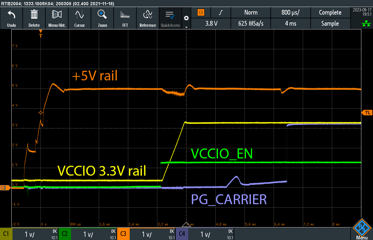
The following scope screenshot shows the power-down sequence when the power switch on the carrier board is cycled from the "on" to "off" position while a lab supply powers the board via screw terminal J1.

In my measurements, the 3.3 V rail ripple was within 5 mVpp.
Scope measurements on the following screenshots were made under the following conditions:
-
The MicroZed is not connected to the carrier board.
-
Jumper JP1 is shorted (to enable the 5 V to 3.3 V regulator).
-
The carrier board is powered from a high-quality lab supply. 5 V via screw terminal J1.
-
A resistor is connected between 3.3V and GND on connector J5.
-
Scope probe 1:1 with short wire ground lead is connected to the VCCIO test point TP9. Scope bandwidth is limited to 20 MHz. AC coupling.
Ripple during 70 mA load on 3.3 V rail:
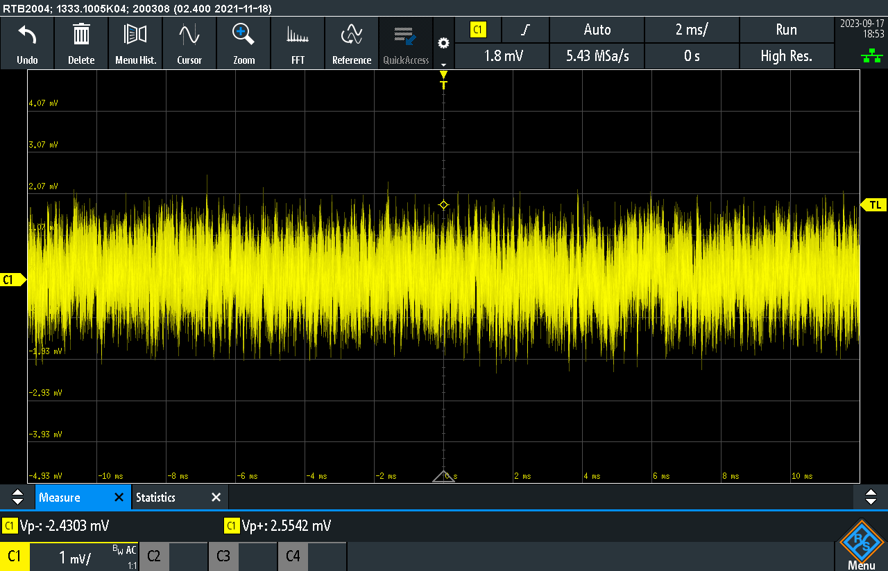
Ripple during 1 A load on 3.3 V rail:

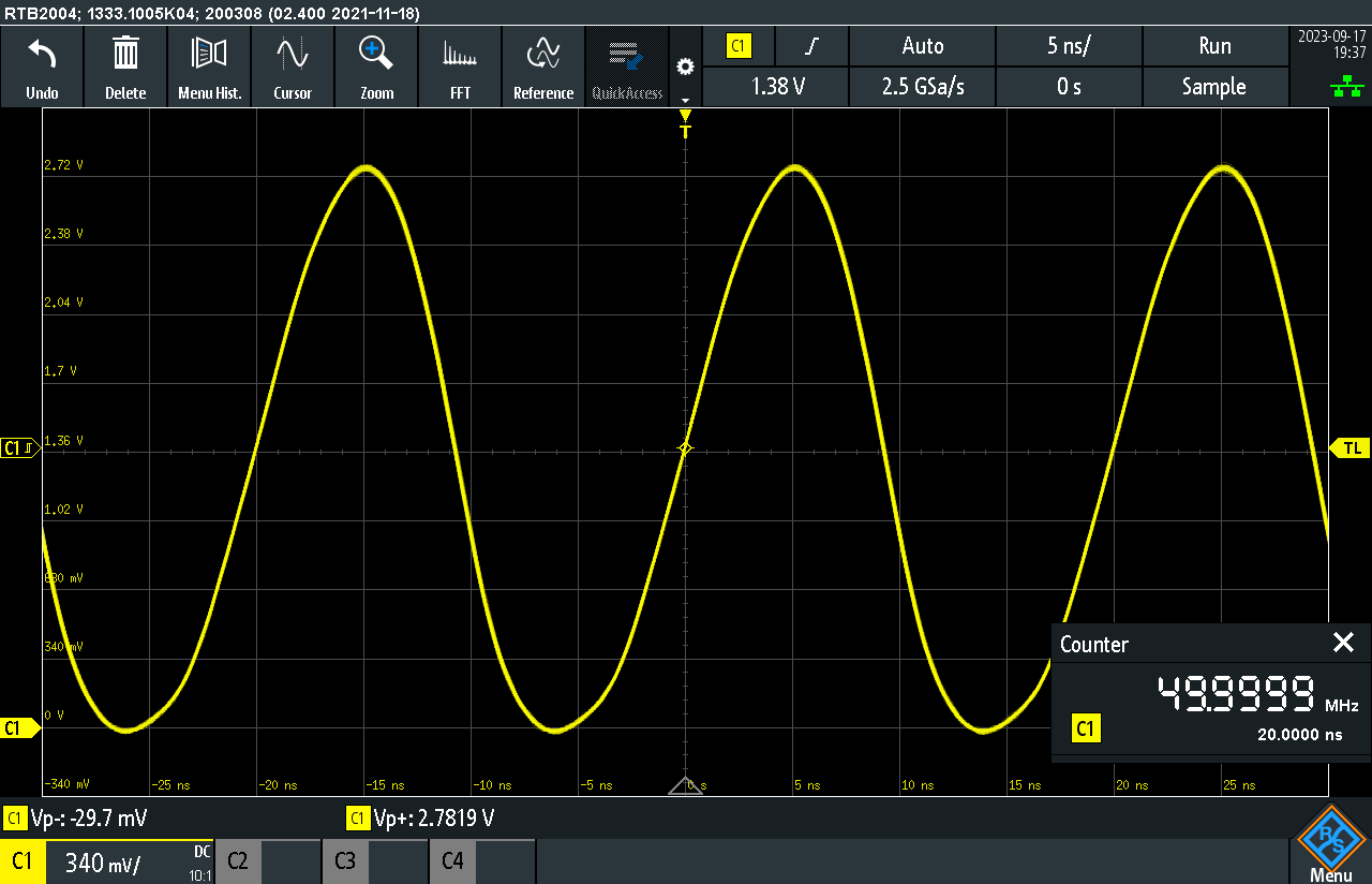
The following scope screenshot shows the oscillator signal on the 50MHz test point TP13. Measured with the MicroZed attached.